Tin is one of the most important functional electroplated coatings in the electronics industry.
Tin is one of the most important functional electroplated coatings in the electronics industry. The reason is the combination of excellent solderability, comparatively low material costs, good electrical contactability, and the ability to deposit fine-crystalline layers with a defined surface morphology. In electronic components, electroplated tin is therefore used on connectors, lead wires, lead frames, passive components, and other contact surfaces, among other applications. Depending on the process parameters, the layer can be adjusted to be matte, semi-gloss, or glossy; key target parameters include wettability, whisker tendency, grain size, internal stress, and layer thickness distribution.
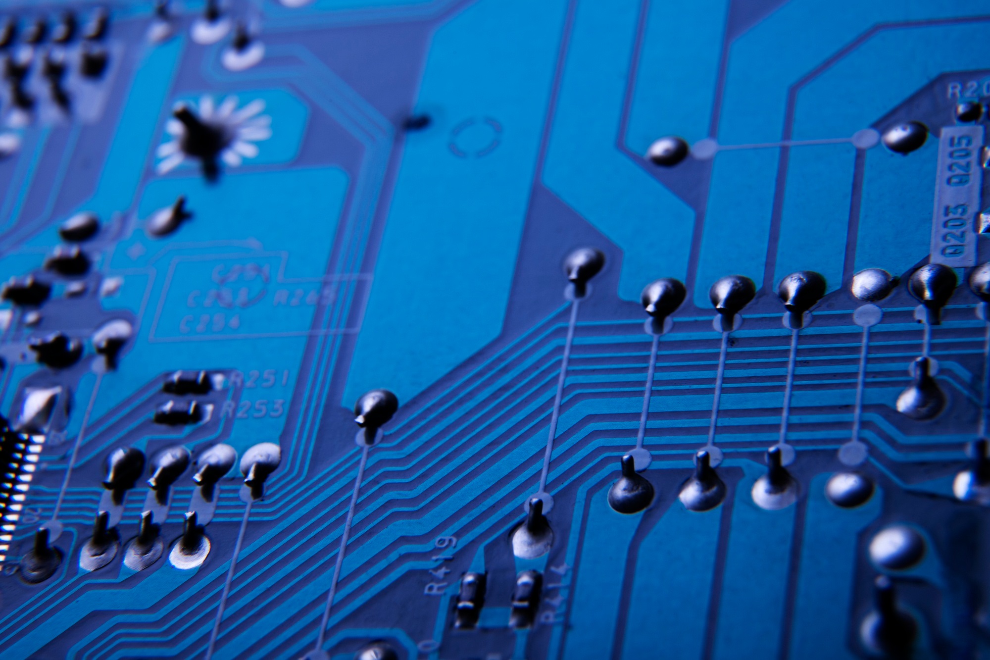
In printed circuit board (PCB) manufacturing, tin serves several purposes. On the one hand, tin or tin-based metal resist is used as an etching resist in outer layer processes: the tin layer protects the desired conductor structures during the subsequent copper etching. On the other hand, tin plays an important role as a solderable final surface, with chemically deposited immersion tin being particularly widespread in the PCB sector today. However, electrolytic tin processes are still used for specific lines and applications. Leading suppliers offer, for example, fine-grained, dense tin deposits with good distribution and suitability for high aspect ratios and blind microvias for PCB metal resist processes, as well as immersion tin as an established end surface for PCBs.
Technologically, the distinction between “matte” and “glossy” is important. Matte tin coatings are usually more finely adjustable, often very robust in terms of soldering, and are frequently preferred where whisker risk, reflow behavior, or defined mechanical properties play a major role. Bright tin is used where a visually brilliant surface, a wide operating range, or specific contact requirements are needed. The exact choice depends heavily on the substrate, line concept, current density window, component geometry, and the requirements for storage stability, solderability, and subsequent processes.
The market for tin-based electrolytes is dominated by suppliers who not only sell raw chemicals but also offer tailored additive systems comprising metal salts, acid components, wetting agents, grain refiners, antioxidants, brightening agents, and post-treatment agents. The following companies are particularly relevant for electronics and PCB applications:
MKS Atotech1
MacDermid Alpha Electronics Solutions2
Technic Inc.3
JCU4
Uyemura5
Qnity Electronics6
Max Schlötter GmbH & Co. KG7
Distinction between bright tin and matte tin
Important note: The exact formulation of commercial baths is generally proprietary. However, publicly available sources allow for a reliable description of the typical composition.
Matte tin – typical bath composition8, 9, 10, 11
A typical matte tin bath consists of:
Matte tin baths are typically designed for good solderability, controlled grain size, low internal stresses, and—depending on the system—reduced whisker formation. Well-known suppliers explicitly describe matte systems as fine-grained, solderable, or low-whisker.
Bright tin – typical bath composition8, 9, 10, 11
A typical bright tin bath contains the same basic components but is more heavily “engineered” with organic additives:
In practical terms, one can say: matte tin is optimized more for microstructure, solderability, and stress levels, while bright tin is optimized more for appearance, gloss range, and surface finish—although modern electronics processes are increasingly combining both sets of objectives.
A technically important distinction is necessary here: In PCB manufacturing, structural through-hole metallization is primarily achieved with copper. Tin plays a role there more as a metal resist or final surface finish. When “through-hole plating” is mentioned in connection with tin, it usually refers to additives that improve wetting, dispersion, coverage, and layer distribution in holes, recesses, or complex geometries—not the actual formation of the conductive through-hole copper wall.
Typical Additives for Grain Refinement8, 9, 10, 11
Publicly described grain refiners or microstructure-controlling additives include, in particular:
In the technical literature, these substances are associated with smaller particle size, smoother surface, better morphology, and, in some cases, altered texture.
Typical Additives for Improved Dispersion / Throwing Power / Wetting8, 9, 10, 11
The following are primarily used to improve dispersion in complex geometries:
The literature and manufacturer sources explicitly describe surfactants as a standard class in tin electrolytes; some suppliers also highlight low surface tension and good performance at high aspect ratios in their PCB metal resist processes.
Additives relevant for vias and deep structures
For vias, through-holes, and other geometries that are difficult to wet, the following are particularly important:
It is precisely in this context that information on tin processes with good coverage, high throwing power, or suitability for high aspect ratios can be found in both scientific review literature and manufacturer specifications.
When distinguishing between formulated additive packages and raw chemicals, the following picture emerges:
Suppliers of formulated process chemicals
The following are particularly relevant for complete process packages including metal salts, acids, additives, analytical services, and technical support:
MKS Atotech1
MacDermid Alpha Electronics Solutions2
Technic Inc.3
JCU4
Uyemura5
Qnity Electronics6
Max Schlötter GmbH & Co. KG7
Typical raw material suppliers for individual chemicals
For individual standard raw materials such as MSA, sulfuric acid, hydroquinone, PEG, or gelatin, traditional fine chemical and distribution companies are often involved, for example:
Bath monitoring is crucial in practice because small deviations in the Sn(II)/Sn(IV) ratio, acidity, chloride, organic additives, or impurities can immediately affect gloss, solderability, coverage, and coating morphology. Typical testing methods include:
Potentiometric Titration
This is one of the standard methods for determining:
Metrohm12 describes this methodology explicitly for acidic and alkaline tin baths.
Typical equipment manufacturers / links:
Metrohm12
Hull Cell Test
The Hull Cell Test is not a substitute for chemical analysis, but a useful process tool. It quickly provides indications of:
The IPC13 test document describes this function in detail.
Typical manufacturers / links:
Kocour14 (Hull Cells)
XRF for coating thickness and composition testing
XRF is widely used in the electronics industry to non-destructively inspect the coating thickness and, in some cases, the composition of finished surfaces and electroplated coatings. This is standard practice for PCBs, lead frames, and connectors. Hitachi High-Tech15 specifically mentions XRF for finished surfaces on PCBs; Bowman and Helmut Fischer offer corresponding measurement systems.
Typical equipment manufacturers / links:
Hitachi High-Tec15
Bowman XRF18
Helmut Fischer19
ICP-OES / AAS / Elemental Analysis
ICP-OES is frequently used for more precise determination of metal content and acid equivalents in more complex baths. Thermo Fisher16 describes the analysis of electroplating baths and the quantification of sulfur as a measure of sulfuric acid.
Typical equipment manufacturers / links:
Thermo Fisher Scientific16
Automated bath analysis / inline or laboratory analyzers
In addition to traditional laboratory analysis, automated bath analyzers are used. With the EBA (Electroplating Bath Analyzer), Technic17 offers a system for simplified and reproducible analysis of electroplating baths.
In practice, the best strategy is usually a combination of:
The PCB market is currently undergoing a visible geographical shift. Drivers include AI servers, automotive/EV, satellite and communications applications, geopolitical risk diversification, and the desire of many manufacturers to reduce their dependence on individual regions. For Southeast Asia—and Thailand in particular—this movement is now more than just a trend.
Thailand has actively supported the PCB sector politically in recent years. According to UNCTAD, in March 2024, Thailand’s BOI incentive framework was expanded to cover the entire PCB supply chain. Concurrently, the BOI reports in its 2025 newsletter on Thailand’s increasingly significant role in the global PCB supply chain. Particularly noteworthy is the momentum in new investments: According to The Nation, in less than three years, nearly 60 PCB manufacturers from China and Taiwan have established new factories in Thailand, including major names such as Unimicron, Zhen Ding Tech, Shennan Circuits, and Victory Giant.
For chemical suppliers, this means that anyone who wants to remain relevant in the PCB industry in the future must not only offer good tin systems but also local technical service, rapid analysis, stable raw material logistics, environmentally compliant formulations, and application-specific additive packages for more sophisticated production line concepts. Consequently, Thailand is attracting not only board manufacturers but also suppliers of equipment, chemicals, and services. For specialty chemical suppliers with expertise in matte tin, bright tin, metal resist, surface finishes, and bath control, this is a clear growth market.